
PCB Design Guidelines #
⚠️ Note: This is a working document I keep for myself to help with design work. YMMV ⚠️
Hi! This resource is something I’ve written for myself over time. I will continue to maintain this and I hope you will benefit from it
Symbol Style Guide #
Here are some style guidelines for creating schematic symbols. Please note that everything is optional (except putting pins on a minimum 100 mil grid), but these suggestions are included to try and make things easier/adhere to best practice
Always check if a symbol already exists, either in our library or on snap eda for import. You can maybe just clean up the snap eda part or upload as is. As much as it would be to have a library with meticulously crafted hand made artisan symbols, sometimes we’re low on time and taking shortcuts is encouraged as long as it doesn’t affect manufacturability/functionality.
| Guideline | Justification |
|---|---|
| Pins should be on a minimum of a 100 mil grid, ideally spaced 200 mil apart. | Putting pins on random grids (or worse, mixing units), means our symbols won’t align in the schematics. 200 mil spacing gives more room for drawing, while 100 mil spacing can be reserved for power pins of the same net, IO banks, and other functional groups that do better compressed |
| Certain components shouldn’t be drawn as a rectangle if they have a common schematic representation. | Op-amps, transistors, switches, oscillators, relays, batteries, and more have a conventional way of being drawn. If you make it a box with pins, the schematic becomes a lot harder to read. Check out wikipedia for some examples: https://en.wikipedia.org/wiki/Electronic_symbol |
| Do not overlap multiple pins of the same function (e.g. GND, VCC, NC) | Doing this obfuscates how things are connected. When debugging you no longer can see which pin is connected to what looking at the schematic. I also often see this cause issues in altium for weird compiler reasons |
| Keep border of component symbols to size small, and fill set to default color (#FFFFB0) | While not necessary, it’s nice to have a unified aesthetic. Makes things look better, especially if we ever have to present the schematics. This is also the default style Altium creates, so it shouldn’t be too onerous. |
| Do not put pins in numerical order, lay them out functionally | Pins should be set up to make your life as easy as possible when drawing the schematic. One symbol can even have multiple variants which are used in different contexts to help keep the schematic readable. |
| Connector symbols should try to represent the physical connector. This can be either a complete mechanical drawing, or by laying out the pins in order | Since connectors have no pin functions, laying them out like the component helps during bring-up/debugging. This way you can look between the schematic and the connector without also switching to layout. |
| Space out power and ground by at least 400 mil. Group power pins of | This spacing allows for decoupling capacitors to be placed in between power and ground, which can make drawing the schematic easier/cleaner |
| Consider drawing the internal schematic of a symbol inside the rectangle if it will help with readability | Some symbols in Altium can end up feeling like black boxes. Drawing the schematic in the symbol can make it clear to future readers of the schematic what is going on without needing to dig into the datasheet |
One more note: Altium also has a symbol wizard for quickly inputting all the pins into a table. This can save time and is worth taking advantage of. You can find it in Tools → Symbol Wizard… or by pressing T, B.
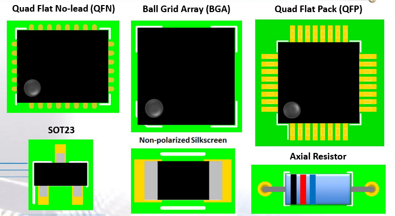
Footprint Creation #
Footprints have a specific naming scheme that IPC has defined. If you use the IPC compliant footprint wizard (see below) this is automatically generated. If not you can take a look at this sheet to see what the name should be. There are some flaws with this naming system. You can read about it here.
Using the IPC Compliant Footprint Wizard
Most components are in standard packages which can work with Altium’s IPC compliant footprint wizard. This will be the easiest way to make new components that have standard footprints.
Altium has already written a guide on how to use it if you’d like.
Footprint Guidelines
| Guidelines | Justification |
|---|---|
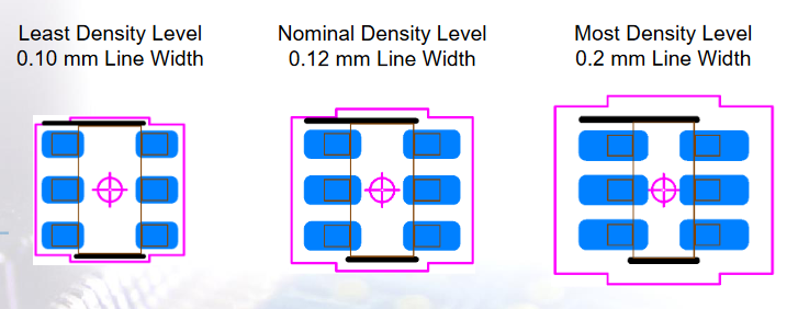
| Courtyard Excess IPC , L (Least), N (Nominal), M (Maximum) Chips Components: 0.10mm, 0.20mm, 0.40mm Electrolytic Capacitors <10mm: 0.10mm, 0.20mm, 0.40mm Electrolytic Capacitors >10mm: 0.20mm, 0.40mm, 0.80mm Standard Chip Components: 0.10mm, 0.20mm, 0.40mm BGA: Dependent on pitch, see linked document pages 26 and 27 |
These numbers come from PCB Libraries, which has a more up to date standard than what’s given by IPC. The three density levels are for the following: Least: Highest density, used for automated assembly processes like reflow + pick and place. Nominal: Medium density, used for hand placed components and reflow Maximum: Used for situations where the components are placed and soldered by hand. (In our lab we probably shouldn’t ever be using this, based on the size of our components) |
| Layer Line Thicknesses Courtyard - 0.05mm Assembly - 0.1mm Silk Screen L (High Density) - 0.1mm N (Medium Density) - 0.12mm M (Low Density) - 0.15mm |
It’s nice to have these be standard across the library. This suggestion is just copying footprint expert, since they’ve spent way more time with pcb footprints than we have. Courtyard and assembly thicknesses are generally less important, but the silkscreen thicknesses should be followed. The minimum silk screen thickness can affect what process the manufacturer decides to use, and could accidentally drive up cost. |
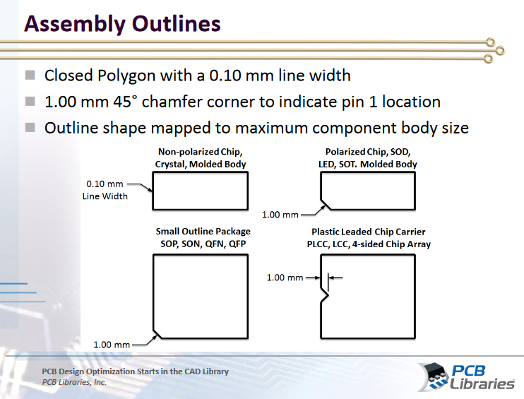
| Mechanical Layers Add component layer pairs for courtyard, assembly, and 3D body on layers 2/3, 4/5, and 6/7 respectively |
All of these layers are useful (courtyard helps with spacing, assembly with bounding boxes/2D collisions, 3D model with collisions and accurate representation. Keeping them on the same layers across components prevents weird Altium issues from arising in the future. That being said, if a layer is labelled as courtyard Altium tries to take care of it in the PCB Layout. Even if they’re on different layers in the components. The issues arise when information is just stored on generic mechanical layers |
| Silk Screen - The silkscreen should be at least the same distance from the copper as it is thick. It should be within the courtyard or sitting on the edge of the courtyard - Please go to this link for examples of how to do pin 1 indicators. I’ve also added a screenshot below. Notion won’t let me include the image in the table :( |
- Using this silkscreen distance is helpful because if you put the silk too close to the pad it will be removed by the manufacturer. This is because if it’s too close to the copper it will just get removed when the solder mask is exposed anyways. Not to mention you don’t want to have the silk on the copper Author’s Note: I prefer this style of pin 1 indicator since it generally takes up less space and pin 1 dots can get confusing. I think these are less likely to accidentally get confused to be assigned to another IC. |
| Pads -If possible use rounded corners on the pads. -Use IPC-7351 to determine pad size, or adhere to manufacturer specific recommendations |
If it’s a straight rectangle it will end up rounding out anyways when it is manufactured. This is also often true of the stencil, and so using rounded pads allows for 100% pad coverage with the solder stencil |
Layout #
Design Rules #
Before you place a single component or route any traces, first you must define the design rules of your board. These rules can be confusing and it’s not always clear what they should be. This next section serves as a guideline, but you might have your own reasons for doing things differently. This won’t cover every rule, but hits most of the ones people have questions about.
| Rule | Description | Recommendation | Justification |
|---|---|---|---|
| Width/ Clearance | Clearance/Width (sometimes called Trace/Space) defines how small (width) and how close (clearance) traces can be. | Width/Clearance limits depend on copper thickness 0.5 Oz - 4/4 mil 1 Oz - 6/6 mil 2 Oz - 8/8 mil |
Going smaller than these values will often increase the cost of the board. If you have a reason to go smaller, check with the manufacturer you want to use on what’s possible with their standard/advanced processes. |
| Solder Mask Expansion | Defines the excess distance around copper pads that should not have solder mask | 1.5 mil recommended Manufacturer/design dependent minimum |
Solder mask expansion is based on the tolerances of the manufacturer’s process. 3 mil will most likely keep the solder mask process as Liquid Photo Imageable (LPI), instead of LDI (Laser Direct Imageable) which is more expensive. The lowest I’ve seen for LPI is 2 mil, but ask your manufacturer if you need tighter tolerances. 1 mil is possible with LDI |
| Hole Size | Defines the minimum drill size | 8 mil recommended 4 mil minimum (check with manufacturer for lower) |
8 mil vias are pretty standard, and going lower may drive up the cost of the board. At a certain point manufacturers need to transition from drills to lasers, which is where the cost comes from. Also please note vias can crack on flex boards, and the risk of cracking is inversely correlated with size. |
| Hole to Hole Clearance | Defines how close drill holes can be to each other | 10 mil | Any lower than 10 mil and you risk cracking or other mechanical defects. This is a hard rule. Please do not go below unless you are 100% confident it won’t cause issues |
| Minimum Solder Mask Sliver | Defines the minimum width a strip of solder mask can be. Sometimes called Solder Mask Dam | Rigid: 4 mil minimum Flex: 6 mil minimum If you want to use lower values please check with the manufacturer |
If this value becomes too small the solder mask will begin to peel off, and that will increase the chances of pads shorting while soldering. Note: we rarely do solder mask in house. However, if you remove this rule you may end up having pads too close together and they might short, so I think it’s worth keeping. |
| Silk to solder mask clearance | Defines the distance from silkscreen to a solder mask opening. Silk needs to be placed on top of soldermask | 6 mil recommended 0 mil minimum |
Generally speaking silkscreen closer than 6 mil to a pad will get removed by the manufacturer. You can leave a note asking them to remove any overlapping silk, or you can set the rule to enforce it for you. Note: we never do silkscreen in house. If you’re making a board internally then this can be ignored |
| Silk to Silk Clearance | Defines how close two separate pieces of silkscreen can be to each other | 0 mil | Who cares if silk overlaps! Go wild with this one. |
| Board Outline Clearance | Defines the distance copper can be from the edge of the board | 10 mil recommended 7 mil minimum |
Having copper too close to the edge can cause issues with shorting due to the tolerances related to depaneling the boards. If there’s copper right at the edge then it will be exposed when the board is cut out. |
| Component Clearance | Defines the distance components should be spaced apart | 0.254mm recommended 0.2mm minimum |
The minimum comes from the highest density courtyard excess. The courtyard encloses the entire component and two components can have courtyards which touch but they should not overlap. It would be nice if Altium had a “courtyards should not overlap” rule, but this will suffice. For instance, you should leave more space around a BGA component to give room for routing. |
Manufacturing Outputs #
Draftsman Documents #
The fabrication and assembly drawings are made in draftsman. Draftsman is Altium’s document editor, and can automatically pull data from the PCB to speed up documentation. Fabrication drawings help coordinate with the manufacturer on things that aren’t described by gerbers. This can include:
PCB Stackup
Instructions on capping/filling vias
Controlled impedance directives
Soldermask color/process (LDI vs LPI)
Fabrication Class (IPC-6012A Class 2 or Class 3)
Assembly drawings help the manufacturer understand what the board is supposed to look like/how the designer intended components to be placed. It can also include instructions such as
How to clean the board after soldering
Which components should be included/not included
Instructions on conformal coating
I recommend generating assembly drawings as they function as a good reference when putting things together. Here is an example from one of our projects
Seeing the designators and pin 1 indicators in front of you without having to go in and out of Altium can save time.
Generating Outputs/Releasing the Board #
Once the board has been designed you need to generate the necessary output files. The required documents are as follows:
Fabrication
GerberX2 or ODB++ files
NC Drill File
Fabrication Drawing
Assembly
BoM
Assembly Drawing
Pick and Place File
IPC-D-356 Netlist
Our Project template helps out with a lot of the process for generating these. Information about what to generate is kept in the outjob files. These can be found in the project files under Settings → Outjob Files.

If you right click on the project you will see an option for the project releaser, which will run through all of the outjob files and generate everything for you.

Releasing a Project #
Congrats! You’ve finished your design! Now it’s time to generate output files and release the project.
Releasing a project is very similar to the processing of tagging something on Git. It creates a point in the commit history where we generated our output files that we can always reference. While rapidly prototyping and fabbing in the lab, this isn’t strictly necessary. But if you send files to a fabrication/assembly house, you will need an easy way to check which version you sent them. And if a change needs to be made in the future, that needs to be tracked. Also having revision numbers on your documentation makes it easy to communicate to manufacturers which version they should be making.
Step 1: Check your work #
Check the following before releasing:
- No schematic errors are left in the electrical rule check (ERC), and all warnings have been waived/deemed acceptable.
- 0 errors appear in the PCB design rule check (DRC)
- Fabrication and Assembly drawings are updated with the most recent design
- Components are in stock/available to you in some way
Also please DO NOT adjust design rules if you don’t understand them. It is your responsibility to understand them and if your design can’t be made with the default rules you can’t always just turn them off.
Step 2: Commit your work #
The project releaser will force you to do this if you haven’t, so you don’t necessarily have to do it manually
Step 3: Release your project #
Right click on your project file and click on Project Releaser
You should then be greeted with the following screen. Ensure the boxes for Include Fabrication Data and Include Assembly Data for ______ are checked.
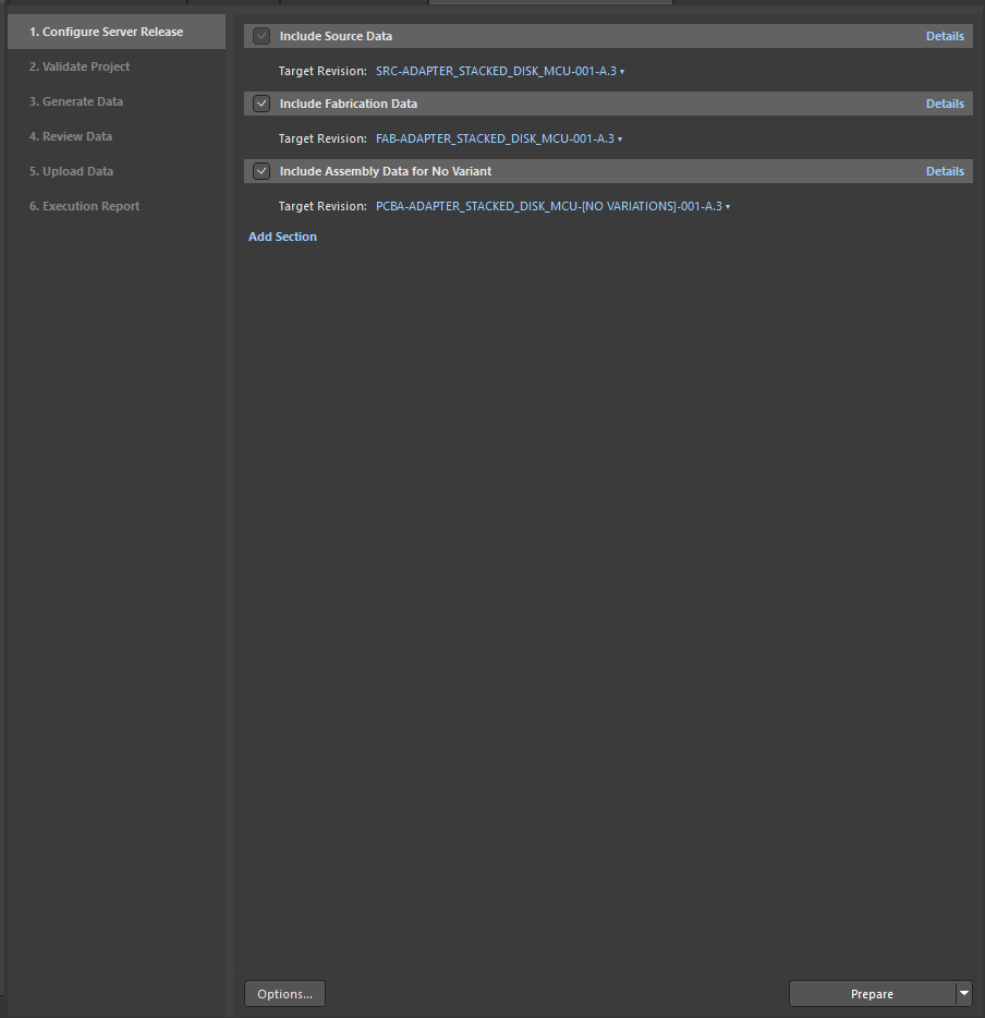
Then press prepare. If all goes well and the above checklist is followed, you should be able to then hit release! If your project fails a design rule check you’ll have to go fix the issues. I know this is annoying especially when the issues aren’t concerning, but this check has saved me from myself too many times to not include.
Once your project is released, you can access the release package online at the 365 workspace (or locally depending on how it’s configured)
Navigate to your project and then go to the releases tab. There you should see your newly released project!
At this point you can download the fab and assembly files to send to a manufacturer. Please note, if you download the full release as one zip, you have to delete the source files before sending it to the manufacturer. Only fab and assembly files should be sent, not schematics and layout.
PCB Design Checklist #
⚠️ Warning: This is constantly being updated/improved ⚠️
A lot of companies will have a design checklist which is given to either the designer or reviewer. It’s meant to help prevent errors systematically by forcing you to check for common issues. This isn’t required, but it might be helpful to have the list. **If you want to use this as a checklist, please copy paste it into your own notion project before checking things off.
Please do not use this religiously or without thought!!!!! This doesn’t cover everything, and you probably don’t need to check everything here.**
For another take on things, feel free to check out this alternative list
Design #
PCB Project #
- Project is saved to our Altium 365 server and is in the correct folder?
- Project parameters are filled out? (Project → Project Options → Parameters)
Schematics #
General #
- Every IC has decoupling capacitors (which meet datasheet recommendations if they exist)
- Components are in stock
- Components are sized appropriately (don’t accidentally pick a 200V 0805 capacitor)
- Pins are all connected to nets or marked as not in use with ERC suppression
- Are any calculations/justifications included in the schematic/linked to from the schematic?
- Components have value, tolerance, package size, and any other relevant parameters displayed in the schematic
- No 4-way junctions?
Power #
- How is power connected to the board?
- Can devices tolerate applied input voltages?
- Has a power budget been made informing battery sizing, regulator sizing, etc. ?
- Can power regulators supply the maximum current of the system?
Microcontroller #
- Is there a way for the microcontroller to be programmed?
- If there’s an external crystal oscillator, are the loading capacitors the correct approximate value?
- Are GPIO or special purpose pins (I2C, SPI, ADC, etc.) assigned correctly based on datasheet pin table?
- Does MCU have any special power requirments (power sequencing, internal regulators, external caps)? Have they been addressed?
- Is there a way to set MCU
High Speed #
- Controlled impedance nets are labelled as such?
- Does antenna have a matching network with plans for how it will be tuned?
Design for Test (DFT) #
- Test pad/pin and debug LEDs included where needed
- If there’s a microcontroller, is there a clear way you intend to communicate with/program it
- Schematic includes documentations/links to any resource used to design the circuit
Layout #
Flex PCB #
- Have traces and board shape, especially near flex points, been rounded/straightened to remove sharp angles? (Sharp angles can create stress concentration areas that lead to fracturing and tearing)
- Has via count been reduced as much as possible?
- Via diameters are are larger than typical rigid board (exact minimum value TBD)
- Has layer count been reduced as much as possible? 1 Layer is great, 2 is tolerable, 4 layer boards are the maximum
- Have regions not designed to flex been protected with stiffener?
- Do all bend radii comply with IPC-2223?
- Are power and signal test points included? (extra useful in case of trace fracture)
- Have solid polygons been changed to hatched polygons where possible? (Helps with flexibility, but keep in mind having a solid ground plane when required)
- Has mechanical mounting strategy been fully planned?
- If you absolutely must solder yourself, have you designed a well rigidized panel with a flat surface layer and alignment features?
- Prefer SMD pads/vias as opposed to N-SMD, or otherwise include extra tabs to keep the copper mecnahically secured in the layer stack. This helps prevent pad rip-up: https://pcbwayfile.s3-us-west-2.amazonaws.com/web/20/07/20/1035048008235t.jpg
- Design rules (width/spacing, impedance, solder mask expansion, etc.) are set up intentionally?
- Pin 1 is clearly marked
- Thermal pads have larger plane underneath for heat dissipation?
- Keep out zones defined and adhered to for mechanically constrained designs?
- DRC passes with 0 errors?
- Analog and digital regions physically separated (but not with split ground planes) if necessary?
- No signals are routed over ground plane splits?
- No vias in flex regions of the board? Or at least stiffener added where said vias lie?
Design for Manufacture (DFM) #
- Stackup is defined?
- Fiducials are placed near BGA/high density footprints?
- Connector pin outs double checked?
Further Resources #
This document cannot cover everything, nor does it intend to. Here are some resources you may find useful related to Altium and PCB design
- Bittele DFM Guidelines: https://www.7pcb.com/Upload_file/DFM_Guidelines.pdf
- Information on defects from assembly
- Altium Beginner Tutorials: https://www.youtube.com/playlist?list=PLXvLToQzgzdfKKQn2wmpuSXz6sROQmO6R
- I like this youtube channel a lot. They cover a lot of important PCB design concepts
- PCB Factory Tour: https://www.youtube.com/watch?v=ljOoGyCso8s